In the semiconductor manufacturing industry, bulk gases are absolutely foundational for critical processes such as deposition, etching, oxidation, and purging. Because even microscopic trace contaminants can induce catastrophic defects or severe yield losses at the nanometer scale, maintaining ultra-high gas purity (often N6 or higher) is a strict requirement. Gases like hydrogen chloride, ammonia, chlorine, and dichlorosilane serve highly specific functions, demanding an analytical system capable of surviving these corrosive and reactive matrices while delivering precise impurity data.
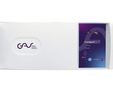
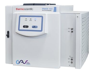
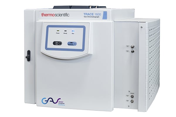
The GAS Semiconductor Industry Gas Analyser is expertly engineered to overcome these exact challenges. Built on the dependable Thermo GC1600 platform, the instrument features an external valve oven housing three specially adapted valves designed with ultra-low leak rates and additional purging capabilities. During operation, a 10-port valve injects the sample and actively backflushes the harsh bulk components to protect the system. Permanent gases and light hydrocarbons are then separated across packed columns before reaching the highly sensitive Pulsed Discharge Detector (PDD). To further protect the instrument’s lifespan, an integrated flush valve drastically minimizes sample contact time. Ultimately, this passivated, highly resilient architecture ensures unparalleled repeatability and detection limits below 20 ppb in a rapid 5.5-minute runtime.
Benefits
Low ppb Detection Limits: Consistently detect permanent gas and light hydrocarbon impurities at ultra-trace levels below 20 ppb, ensuring absolute quality control of critical bulk gases.
Robust Design for Aggressive Gases: Expertly constructed to withstand highly corrosive and reactive gas streams by utilizing fully passivated components and a dedicated flush valve to safely minimize chemical exposure.
High Repeatability: Delivers highly dependable, consistent analytical results with exceptional repeatability measuring below 1% RSD, guaranteeing strict process stability.
Fast Analysis Time: Maximizes laboratory and operational throughput with a highly optimized analytical runtime of approximately 5.5 minutes, providing rapid feedback for continuous process monitoring.
Low Maintenance Operation: Incorporates a modular iConnect injector and detector concept paired with specialized low-leak valves to ensure high system uptime and simplified routine servicing.
| Category | Specification |
|---|---|
| Analyser Platform | Thermo GC1600 with external valve oven |
| Detector Type | Pulsed Discharge Detector (PDD) |
| Injection System | Modular iConnect injector concept with highly adapted, low-leak valves |
| Valve Configuration | 3 specially adapted valves (including two 10-port valves and a flush valve) |
| Column Setup | Packed columns featuring automated bulk component backflushing |
| Sample Pathway | Fully passivated sample-wetted parts to resist highly corrosive media |
| Target Components | Permanent gases and light hydrocarbons in bulk aggressive gases (e.g., HCl, HBr, BCl₃, Cl₂, NH₃, CF₄, NF₃, N₂O, DCS) |
| Limit of Detection (LOD) | < 20 ppb |
| Repeatability | < 1% |
| Analysis Runtime | 5.5 minutes |
| Software System | Chromeleon chromatography data system |
Bulk Gas Purity Control: Accurately analyze trace impurities within aggressive process gases to guarantee the integrity of critical semiconductor fabrication workflows.
Etching and Deposition Processes: Continuously monitor the absolute quality of highly reactive and corrosive gases directly utilized in sensitive wafer manufacturing steps.
Ultra High Purity Gas Verification: Thoroughly verify that incoming and utilized gases meet stringent N6 (6.0) or higher purity specifications to proactively prevent costly yield losses.
Semiconductor Manufacturing Facilities: Provide essential analytical support to ensure the stable, uninterrupted operation of delicate semiconductor and microelectronics fabrication environments.
Process Development and R&D: Empower research initiatives and the development of next-generation semiconductor processes through highly accurate, trace-level impurity profiling.
Designed to continuously verify and strictly maintain N6 (6.0) or higher purity levels demanded by modern semiconductor manufacturing and high-precision wafer fabrication regulations.